Technological advances on the treatment of Si-kerf, graphite and silica waste streams for the PV industry
Written by RESITEC
1. Introduction and summary
1.1 Purpose of the document
The photovoltaic industry is one of the most mature among the renewable energy sources and is considered essential within the green shift. The total capacity installed surpassed 1 TW in 2021, see figure 1 [International Energy Agency, 2022], and further growth is needed to be 25% per annum until 2030 for the Net Zero Emissions (NZE) by 2050 Scenario [International Energy Agency, 2021]. Such a growth of the industry will generate larger amounts of waste materials throughout the whole value chain. To ensure sustainability it is necessary to find adequate processing solutions and applications for all the waste streams generated in the value chain, thereby avoiding both landfills and losses to wastewater. The focus in this work (ICARUS – WP2) has been on the waste materials generated from the ingot manufacturing- and the wafering- steps in the value chain. There are two main waste streams for the ingot manufacturing, these are;
1) silica crucibles with remaining silicon melt (silica crucible waste) and
2) worn-out graphite from the hot-zone
3) silicon kerf from wafer sawing
While the silica crucibles crack upon cool down, due to the phase change occurring from b-cristobalite (in inner layer) to a-cristobalite, which is accompanied by a volume change of 5% [Thorsen et al., 2016]. Therefore, silica crucibles are discarded after each furnace run, while the graphite parts are changed less frequently. Thus, the volumes generated of silica crucible waste are much larger than the volumes of graphite. Estimations from the crystal grower in the project indicate that the amounts of silica crucible waste are roughly four times higher than the amounts generated for graphite scrap materials. For the wafering step there is one main waste material generated and this is silicon kerf, see figure 2 (right). In terms of volume, it is the most significant waste material from the ingot manufacturing and wafering processes. The volumes generated yearly are estimated to more than 2×10⁵ MT from 2021 [Blömeke et al., 2023 and Ji et al., 2023]. As a key element for the transition to low-carbon energy systems silicon has been classified as a critical raw material by EU since 2014 [Bobba et al., 2020]. This highlights further the importance of developing efficient processing lines for silicon waste streams.
The purpose of this document is therefore to give a status on the technological progress within the recycling of the three waste streams from the ingot- and wafer-manufacturing: silicon kerf, graphite and silica. Both the processing routes established for the materials and first results from the testing into different applications are reviewed.
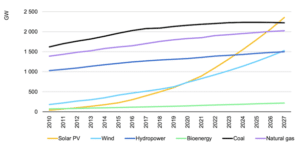
Figure 1: Cumulative power capacity, gigawatts (GW), by technology, 2010-2027. Source: IEA Renewables 2022.
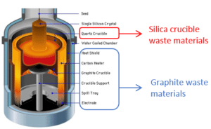
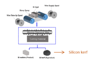
Figure 2: (Top) Waste streams generated from ingot manufacturing – (Bottom) wafering- steps (figure from: Li et al. 2021) in the photovoltaic value chain
1.2 List of definitions, acronyms and abbreviations
ICP-MS Inductively coupled mass spectrometry
BET Brunauer-Emmett-Teller
NZE Net Zero Emissions by 2050 Scenario
IEA International Energy Agency
Cz Czochralski
DWS Diamond wire sawing
LAS Loose abrasive sawing
SEM Scanning electron microscopy
SEI Solid electrolyte interphase
LIB Lithium-ion battery
XRD X-ray diffraction
LECO Carbon combustion analyses
LDP Laser diffraction particle size analyses
1.3 Structure
This document is structured as follows:
- Section 1 Introduction and purpose: gives an introduction/motivation to the subject and the purpose of this document
- Section 2 Silicon kerf: comprises a background followed by characteristics of the silicon kerf, processing routes explored including treatments developed for special applications, and preliminary results from testing downstream
- Section 3 Graphite: comprises a background, sorting and collection strategy, characterization, processing routes explored, preliminary results downstream
- Section 4 Silica crucible waste: comprises a background, collection and processing route established, review of results from the testing downstream
- Section 5 Conclusions: summarizes the main technological achievements and potentials with regards to applications
1.4 Relationship with other documents
This document complements the following deliverables:
- D1.2: Public initial waste inventory
- D2.7: Purification strategy and quality requirements for the treatment of Si-kerf, graphite and silica waste streams
- D6.10: Electrochemical properties of recycled graphite and silicon
- D6.11: Recycled graphite as anode material
2. Silicon kerf
2.1 Background
Silicon kerf is generated during the diamond wire sawing (DWS) of blocks into wafers. The amounts of silicon kerf formed are correlated to the diameter of the wire (see figure 3, [Kong et al., 2021]) and to the cutting technology. The transition from loose abrasive sawing (LAS) with silicon carbide particles as the abrasive medium, to DWS, has allowed smaller diameters on the wire and faster cutting speeds [Wallburg et al., 2022]. The amounts of silicon kerf generated can be reduced with DWS dependent on the sawing parameters applied (wire diameter, travel velocity of wire, diamond size, etc.) [Seeholzer et al., 2021 and Ryningen et al., 2020].
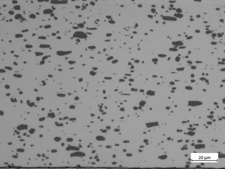
The silicon kerf particles are characterized by a flake-like morphology as visualized in figure 4. The particle size distribution as measured by laser diffraction shows a d50 ~ 700 nm, but due to the anisotropic shape should be considered together with the Scanning Electron Microscopy (SEM) imaging. The main impurities in the slurry recovered after the DWS process are nickel from the nickel-plated diamond wire, aluminum from the base plate material and different organic compounds from the cutting fluid and beam plate material in use [see Icarus reports D1.2 and D2.7]. The level of aluminum can vary significantly between different producers dependent of the base materials in use, see figure 5, since some wafer producers employ base materials without Al(OH)3 as a component in the base materials. The nickel contents are however more stable between the different producers and range around 50-200 ppmw.
Following the transition from LAS to DWS the recycling of silicon kerf has clearly benefited from the fact that the slurry after wafering now contains only silicon as main solid and no silicon carbide. However, still remaining substantial challenges are the high moisture contents, small particle size with correspondingly high surface area and residues of organic substances from the cutting fluid. These factors make the particles very reactive and pose significant safety concerns for the material processing.
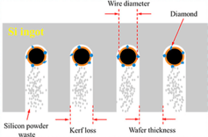
Figure 3: Figure adapted from Kong et al., 2021, detailing the DWS process
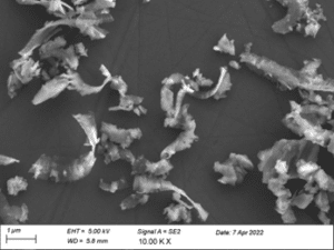
Figure 4: Scanning electron microscopy (SEM) image of silicon kerf particles
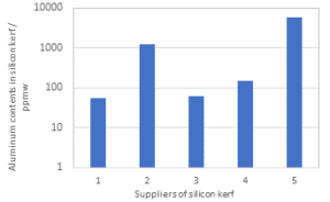
Figure 5: Contents of aluminum in silicon kerf from different suppliers measured by ICP-MS
2.2 Collection of the silicon kerf at the wafer producer
When cutting the silicon wafers in a diamond wire saw a cutting fluid is used. This is normally water with a small amount of organic additives. There is a tank with cutting fluid under each saw and the fluid circulates over the ingot to cool and remove fine silicon from the kerf made by the wire. After each cut the cutting fluid has reached a fine solid level of around 4 % and is then being changed.
The spent fluid from each saw is pumped to a filtering system where the fine solid is separated from the liquid. The filtration is normally done with a filter press specially designed filtration of very fine solids. The solid filter cake (see figure 6) with a humidity level of around 40 % by weight is removed from the filter and packed in big bags at the wafer producer. The clear filtrate liquid can be reused or goes to effluent.
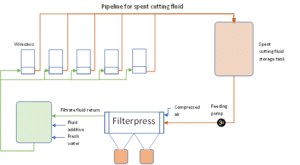
Figure 6: Simplified flow sheet for wire saw cutting fluid filtration for collection of silicon kerf filtercake
2.3 Process routes for silicon kerf filter cake material
In the ICARUS project the silicon kerf goes from PILOT A (RESITEC) to different downstream applications. It goes both directly to end application and to the other pilots (PILOT B, C), see figure below.

Figure 7: Overview of silicon kerf flow from Pilot A and targeted application
As a consequence of this there needs to be specific processing for some of the applications. Different requirements are needed for the product to go into, for instance PILOT B where it will be subjected to further refining through several steps, then into thermoelectric modules, where it goes directly into the end applications. Therefore, different industrial scale processes have been developed and tested, as well as pilot-scale processing, and how to combine these depends on the downstream usage.
2.4 Drying of filter cake material
After the filtering of the slurry containing silicon kerf the material still contains a high amount of moisture, typically ranging from 30-50%. Figure 8 shows a typical filter cake material. The drying constitutes a crucial step in the treatment of silicon kerf. Since the silicon kerf particles are small and have a relatively high surface area combined with the high affinity that silicon has for oxygen, the drying step poses both safety and quality concerns. The water molecules have the ability to oxidize the silicon according to the reactions given below.
Si(s) + 2H2O(l) = SiO2(s) + 2H2(g) ΔHr0= -339 kJ/mol at standard state conditions (1)
Si(s) + 2H2O(g) = SiO2(s) + 2H2(g) ΔHr0= -427 kJ/mol at standard state conditions (2)
During the drying process it is important to control these reactions to avoid large amounts of hydrogen gas evolving, in addition to limiting the oxidation of the silicon kerf particles. For most of the downstream applications under testing in the ICARUS project the oxide layer thickness on the silicon kerf particles should be as narrow as possible.
ReSiTec has developed an industrial scale batch drying process and has installed and commissioned a continuous drying equipment for silicon kerf, see figure 9 of the continuous dryer below. For the required security level several safety measures have been implemented, as for example the monitoring of heat evolution with permanent thermal camera installations, and the in-line measurements of other critical parameters for the safety and control of the process. Capacities obtained are increased compared to the batch process. A moisture level of < 1% has been obtained for the silicon kerf.
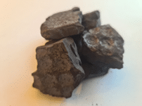
Figure 8: Image of filtercake material before drying
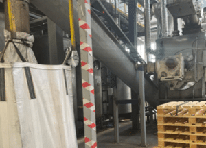
Figure 9: Continuous drying equipment for installed at ReSiTec
2.5 Purification of filter cake material
The main impurities for the silicon kerf are foreign particles coming from the beam materials and the nickel-plated diamond wire, as well as remnants of the cutting fluid. An industrial scale purification process based on acidic treatment has been developed which is particularly efficient in the reduction of aluminum, nickel and iron, see figure 10. A second purification method (secondary treatment) has been tested in lab/pilot-scale for the reduction of carbon. With this method it is possible to reduce the carbon contents down to < 0.25 ppmw.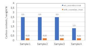
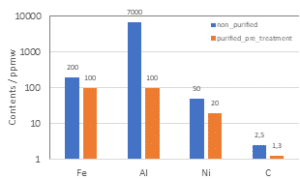
Figure 10: Analyses of silicon kerf filter cake subjected to different purification treatments a) GDMS measurements after purification b) LECO measurements after secondary treatment
2.6 Deagglomeration and post treatment of silicon kerf filter cake
Depending on the targeted application it can be necessary to have the material in a powder form where the silicon kerf particles are as separated as possible. An industrial scale process for the has been developed and tested for the deagglomeration of the silicon kerf filter cake. Special safety measures are necessary also here due to the small particle size and the high affinity to oxygen that silicon possesses, together with the risk of dust explosions. Optimizations on the equipment to increase the efficiency of the process have been installed and tested, showing good overall improvements.
2.7 Targeted processes for lithium-ion battery (LIB) application and thermoelectric modules
For some targeted applications, such as the lithium-ion battery (LIB), surface characteristics of the particles have particular importance. Formation of solid electrolyte interphase (SEI) leads to large losses in the capacity and is particularly pronounced for silicon (f.ex. Shin et al., 2020, Pinson et al. 2013, Vorauer et al., 2023). Specific surface treatments/coatings may protect the silicon and reduce the losses due to SEI formation and can in addition help in keeping the integrity of the particles. Several different treatments of silicon particles have been and are being tested. A few have so far been identified as promising with regards to cycling stability and further studies on these treatments are ongoing.
In addition to surface properties a particle size below ~150 nm can improve the cycling stability of silicon in LIB since the expansion of the silicon upon lithiation will not lead to disintegration of the particle (Liu et al., 2012, Asenbauer et al., 2020). Although the thinnest side of the silicon kerf particles are only a few tens of nanometres the length of the particles can extend up to a few micrometres. Experiments with milling of silicon kerf in an agitator bead mill down to around 100 nm (d50) have been conducted, figure 11. The milling time was like silicon powder of similar size, but with more spherical/isotropic shape. The milled silicon kerf material is being tested in half coin cells and will be compared to non-milled material.
For the testing of silicon kerf into thermoelectric modules different processing routes have been explored. These are both with and without purification and including deagglomeration. The results show that more important than purity is the conductivity type, where the most promising results were obtained on n-type silicide [Mangelis et al., 2023].
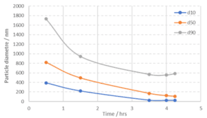
Figure 11: Particle size as a function of milling time from experiments with milling of silicon kerf
3. Graphite
3.1 Background
The Cz-furnace is the base equipment for pulling monocrystals of silicon for the photovoltaic industry. A central part of the furnace is the hot-zone which is made up of different high quality graphite elements. The hot-zone is often specially designed and a part of the intellectual property of the manufacturer. The different parts of the hot-zone are exposed to both high temperatures and SiO, CO and Si gases formed inside the chamber. At regular, but different intervals, the parts will have to be exchanged. Graphite is therefore a significant waste material in the production of monocrystalline silicon. To be able to recycle these graphite parts back into new graphite products is a clear target.
3.2 Characterisation of worn out hot zone parts
Some of the specially designed and machined graphite elements will show higher wear rate than others due to variations in exposure to heat radiation, temperatures, and gases. A thorough characterization of graphite elements from eight different parts of the hot-zone has been conducted. Ash contents both at the surface and in bulk have been measured, depth of surface layer, as well as characterization of the microstructure, see table 1 below for summary of the results.
Table 1: Characterisation of worn-out graphite elements from the hot-zone
| Graphite element | Ash contents surface / wt% | Ash contents bulk / ppmw | Depth of surface layer / mm | Microstructure type |
| 1 | 10 | 636 | Isotropic | |
| 2 | 207 | Isotropic | ||
| 3 | 11 | 1097 | 270 | Regular |
| 4 | 2.9 | 54 | Isotropic/Regular | |
| 5 | 5.4 | 460 | Isotropic | |
| 6 | 14 | 18 | 230 | Isotropic |
| 7 | 5.5 | 1105 | 300-1300 | Isotropic |
| 8 | 4.4 | 302 | 5 | Isotropic/Regular |
From the characterization of the different graphite elements it is observed that the ash contents both on the surface and bulk vary significantly, ranging between 2.9 to 14 wt% in the surface and from 18-1105 ppmw in the bulk. The depth of the surface layer is mostly below 1 mm. The deposited layers consist of either crystalline SiO2, SiC and Si phases or a mix of these phases (see report D1.2). Although for most elements the microstructure is isotropic there are some elements that show more oriented structure (regular), see figure 13. The large inhomogeneity in the worn-out graphite elements increases the complexity for the recycling of these parts.
3.3 Collection of materials
A sorting strategy based on visual observations was implemented at the supplier for the collection of the materials, see figure 12 These were sorted into three categories 1-3 with increasing purity from 1 to 3, where no deposits were observed for category 3 materials.
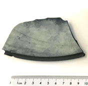
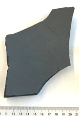
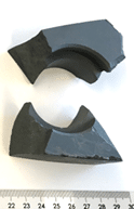
Figure 12: Sorting categories for the graphite waste materials (Categorie 1, Categorie 2, Categorie 3)
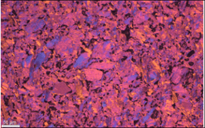
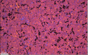
Figure 13: Micrographs from characterization of hot-zone elements, a) element 2 showing an isotropic structure and b) element 3 showing a regular structure
3.4 Processing of graphite waste materials to LIB application
Graphite as anode material for LIB must fulfill a range of strict requirements with regards to purity, surface area, particle size distribution, tap density. For the processing of graphite waste material, the graphite elements from the purest category were selected, which was category 3. A combination of crushing, milling and sieving has been tested out to achieve the correct particle size distribution. Both ball milling with tungsten carbide balls and jet milling were considered as milling methods. Trials resulted in suitable particle size distributions, but the latter method led to lower impurity levels, see table 2. Although jet milling requires high energetic input, it is preferred, as this technique offers ultra-high purity conditions, since there are no mechanical griding parts, and can result in less contamination as was observed in the testing. For the processed graphite waste material, the resulting particle size distribution was within specification, but the specific surface area was too high, this was however effectively reduced to 1 m2/g with a combination of additional classification to decrease the amounts of fines and coating of the particles. Testing of the materials produced in half coin cells has shown that the performance is much lower than expected for graphite anode materials (see report D6.11). This could be due to amongst other the higher impurity contents still obtained after jet milling which may be caused by the initial contents in the material, in addition to the crushing in jaw crusher of the larger elements. Another reason for lower capacities could be the degree of graphitization of the material, but additional analyses would be necessary for clarification.
Table 2: Analyses of ball milled and jet milled graphite from category 3
| Analyses / ICP-OES / BET | Ball milled graphite | Jet milled graphite |
| S / % | < 0.1 | <0.1 |
| Al / ppmw | 77 | 35.5 |
| Ca / ppmw | 98.7 | 356 |
| Co / ppmw | 26.6 | < 0.1 |
| Fe / ppmw | 84.7 | 44.4 |
| Ni / ppmw | 3.6 | < 0.1 |
| Si / ppmw | 829 | 334 |
| Ti / ppmw | 6.8 | 16.7 |
| W / ppmw | 165.8 | < 0.1 |
| Ash content / % | 0.24 | 0.16 |
| Specific surface area / m2/g | 13 | 7 (uncoated) and 1 (after coating) |
3.5 Processing graphite to applications like bipolar plates or closed loop isostatic graphite production
For processing of graphite to the applications bipolar plates for fuel cells and closed-loop isostatic graphite production both category 1 and 2 has been considered. A different processing route has been established than for the application to LIB since larger volumes are necessary for the testing downstream. The initial crushing of the large graphite elements has however been identical. For the milling of the material a pilot-scale proprietary rod mill has been applied, see figure 14. The milling of graphite is challenging as the material is soft and easily can coat the rods. However, after optimizations of the processing route it has been possible to obtain the targeted particle size distributions and ash contents (0.07 wt% and 0.14 wt%) for the material to be tested downstream, see figure 15.

Figure 14: Simplified flow sheet for graphite waste processing
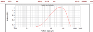
Figure 15: Particle size distribution as measured by laser diffraction for graphite waste material processed after route in figure above
4. Silica crucible waste
4.1 Background
The crucibles used in the Cz-process for manufacturing of monocrystalline silicon ingots are made from high purity amorphous quartz (total impurities < 30 ppmw) to avoid contamination of the silicon [Roberts, 2012]. Due to the manufacturing process, they contain many bubbles, therefore they have two layers; an outer thicker layer with bubbles, and an inner bubble free layer facing the silicon melt to avoid bubbles from entering the molten silicon which can induce structure loss. During the furnace cycle the amorphous a-quartz transforms to b-cristobalite for the inner layer at high temperature, and then to a-cristobalite when the temperature drops below 280 °C. This last phase change is accompanied with a volume decrease which causes the cracking of the crucibles [Thorsen, 2016]. The crucibles always contain a residual silicon melt after the pulling of the monocrystals which remains in the crucibles upon cool-down, see figure 16. The crucibles with residual silicon are discarded after each furnace run, this remaining silicon is the so-called “pot-scrap”. This silica crucible waste is therefore a mixture of silica and silicon. Targeted applications within ICARUS are PILOT B, metallurgical silicon production in an arc furnace, and silicon carbide production, see figure 16. One is a direct route and will consequently imply stricter requirements for the processing route of the silica crucible waste.
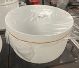
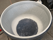
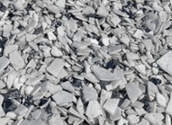
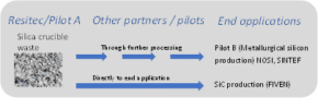
Figure 16: a) Crucible before furnace run b) Crucible after furnace run with remaining silicon (pot-scrap) c) Silica crucible waste as received @ ReSiTec d) overview of applications intended for processed silica crucible waste
4.2 Processing, characterization and testing of silica waste stream
To avoid contamination of carbon materials a specific sorting regime was implemented at the supplier before discarding the silica crucible waste materials. A processing route like that for the graphite scrap materials was adopted; including crushing, milling and sieving as the main steps. Since both the silicon and the silica are brittle materials fines (particles < 75 mm) are easily generated in the crushing and milling of the materials. For the intended applications the amounts of fines are critical due to both dusting and furnace operations and should be as low as technically feasible. Several campaigns with production of materials for testing in silicon carbide production has been run, the amounts of fines have been significantly reduced compared to first campaign and a suitable particle size distribution has been obtained for the material. Production of high purity silicon carbide for the semiconductor industry requires a highly pure silica feedstock material and particularly aluminum can be critical. The processed silica waste materials has been analyzed with ICP-MS, which shows that the aluminum level can be kept below 20 ppmw. This yields a sufficiently low aluminum level in the resulting silicon carbide to qualify as a high purity grade. Although the levels of iron and nickel are high in the processed silica crucible waste materials, this element is efficiently reduced in the process for production of silicon carbide. The contents of dopants; boron, phosphorus and gallium come from the silicon part. As the industry is moving towards gallium as a p-type dopant rather than boron, the silica waste materials will be dominated by gallium in the future. X-ray diffraction analyses of the feedstock confirm, as expected, that the silica part of the processed waste materials is mainly amorphous silica with a smaller amount of cristobalite, see figure 18. Results from the testing of the feedstock material from the established processing route for silica waste materials at ReSiTec, into silicon carbide production, show high yields in the process, if amounts of fines are kept low enough, and that the silicon carbide produced is of high purity grade. Preliminary test results from the use of the produced feedstock material from silica waste materials at ReSiTec, into metallurgical silicon production, are also promising with high yields observed, the material quality remains to be verified.
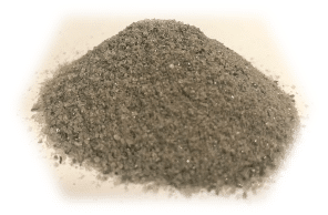
Figure 17: Silica waste materials after sorting and processed through established pilot processing route at ReSiTec
Table3: ICP-MS analyses of silica waste materials sorted and processed through established pilot processing route
| Element / ppmw | Processed silica waste materials 1 | Processed silica waste materials 2 |
| Boron | < 0.8 | < 0.73 |
| Aluminum | 17 | 17 |
| Titanium | 2.2 | 2.1 |
| Iron | 555 | 279 |
| Nickel | 57 | 25 |
| Gallium | 63 | 86 |
| Phosphorus | 4.2 | 4.3 |
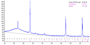
Figure 18: XRD measurements of silica waste materials sorted and processed through established pilot processing route
5. Conclusions
Industrial scale processing routes for all three waste materials have been established at ReSiTec, including a sorting and collection strategy. Materials produced have been tested into various downstream applications, both directly to end application and to other pilots in the project. A continuous drying equipment has been successfully commissioned and tested as an alternative to the current batch drying process for silicon kerf filter cake, yielding moisture levels < 1 wt%. A dedicated industrial scale deagglomeration process has been developed and tested as well as a purification process bringing down particularly aluminum, nickel and iron. Processes for surface treatments and particle size reduction of silicon kerf specifically intended for testing as anode material in LIB are being explored. Preliminary results from the testing of surface treated silicon kerf into LIB and testing of silicon kerf deagglomerated into thermoelectric modules, are promising.
For the graphite waste materials characterization of different parts from the hot-zone shows a large inhomogeneity in the materials with regards to ash contents and surface deposits depth, which adds complexity to the recycling of this waste stream. Processing routes in pilot scale for the different categories of graphite waste materials have been developed and tested. Main processing steps involved are crushing, milling and sieving, including both rod-mill and jet-mill technologies. While the testing into the applications bipolar plates or isostatic graphite is ongoing, the preliminary results from testing into anode in LIB show both substantially lower capacity and cycling stability than benchmark graphite. Different properties of the recycled graphite, as for example purity or graphitization degree, may be limiting factors.
For silica waste materials, a specific collection and pilot-scale processing route has been established and optimized. Particularly the contents of fines were reduced for the product stream, which is important for the downstream applications. Testing of the feedstock produced into silicon carbide production shows very high yields and the resulting silicon carbide is of high purity grade. The possibility for running an upscaled (industrial-scale) testing of the feedstock material from processed silica waste materials, into silicon carbide production, is currently being explored. For metallurgical silicon production in pilot B the feedstock material from processed silica waste materials has been tested. Initial results are also here promising showing high yields, the quality of the silicon produced is under assessment.
References
1 International Energy Agency, “Net zero by 2050 A roadmap for the global energy sector”, 2021, https://www.iea.org/reports/net-zero-by-2050
2 International Energy Agency, “Renewables 2022 Analysis and forecast to 2027”, 2022, https://www.iea.org/reports/renewables-2022
3 J. Li, Y. Lin, F. Wang, J. Shi, J. Sun, B. Ban, G. Liu, J. Chen, “Progress in recovery and recycling of kerf loss silicon waste in photovoltaic industry”, Separation and Purification Technology, Volume 254, 2021
4 J. Kong, D. Wei, P. Xing, Y. Zhuang, S. Yan, “Recycling high-purity silicon from diamond wire saw kerf slurry waste by vacuum refining process”, Journal of cleaner production, Volume 286, 2021
5 S. Blömeke, R. Arafat, J. Yang, J-P. Mai, F. Cerdas, C. Herrmann, “Environmental assessment of silicon kerf recycling and its benefits for applications in solar cells and Li-ion batteries”, 30th CIRP Conference on Life Cycle Engineering, Procedia CIRP 116 (2023) 179–184
6 F.W. Thorsen, “Investigation of quartz crucibles for monocrystalline silicon ingots for solar cells”, Master of science in mechanical engineering, NTNU, 2016
7 H. Ji, Z. Liu, X. Li, J. Li, Z. Yan, K. Tang, “Recycling silicon waste from photovoltaic industry to prepare yolk-shell Si@void@C anode materials for Lithium-ion batteries”, Processes 2023, 11, 1764
8 S. Bobba, S. Carrara, J. Huisman, F. Mathieux, C. Pavel, “Critical raw materials for strategic technologies and sectors in the EU”, 2020, doi: 10.2873/865242
9 F. Wallburg, M. Kuna, M. Budnitzki, S. Schoenfelder, “A material removal coefficient for diamond wire sawing of silicon”, Wear, volumes 504-505, 2022
10 B. Ryningen, P. Tetlie, S. Gulliksen Johnsen, H. Dalaker, “Capillary forces as a limiting factor for sawing of ultrathin wafers by diamond-wire saw”, Engineering Science and Technology, Journal 23, 2020, 1100-1108
11 Icarus report D1.2, “Public initial waste inventory”, 2022
12 Icarus report D2.7,”Purification strategy and quality requirements for the treatment of Si-kerf, graphite and silica waste streams”, 2022
13 L. Seeholzer, S. Süssmaier, F. Kneubühler, K. Wegener, “Experimental investigation of the machining characteristics in diamond wire sawing of unidirectional CFRP”, The international journal of advanced manufacturing technology, volume 117, 2197-2212, 2021
14 J. Roberts, “High purity quartz: Under the spotlight. Industrial Minerals, 2012. Downloaded 13.06.16 from: http://search.proquest.com/docview/993118306?accountid=12870
15 J. Shin, T-H. Kim, Y. Lee, E. Cho, “Key functional groups defining the formation of Si anode solid-electrolyte interphase towards high energy density Li-ion batteries”, Energy Storage Materials, Volume 25, Pages 764-781, 2020
16 M. Pinson, M. Bazant, “Theory of SEI formation in rechargeable batteries: capacity fade, accelerated aging and lifetime prediction”, Journal of the Electrochemical society, 160 (2) A243-A250, 2013
17 T. Vorauer, J. Schöggl, S. G. Sanadhya, M. Poluektov, W. D. Widanage, L. Figiel, S. Schädler, B. Tordoff, B. Fuchsbichler, S. Koller and R. Brunner, “Impact of solid-electrolyte interphase reformation on capacity loss in silicon-based lithium-ion batteries”, Nature Communications Materials 4, Article number 44, 2023
18 X.H. Liu, L. Zhong, S. Huang, S. Mao, T. Zhu, J.Y. Huang, “Size-dependent fracture of silicon nanoparticles during lithiation”, American chemical society nano, 6, 2, 1522-1531, 2012
19 J. Asenbauer, “The success story of graphite as lithium-ion anode material – remaining challenges and recent developments including silicon and silicon (oxides) composites”, Sustainable Energy Fuels, 4, pages 5387-5416, 2020
20 P. Mangelis, A. Sousanis, G. Mesaritis, P. Ioannou A-K. Søiland, Y. Xu, T. Kyratsi, “High thermoelectric performance of Mg2Six-0.03Sn1-xBi0.03 (x=0.4, 0.6) based on recyclable Si-kerf from PV manufacturing”, presentation for the 19th European conference of Thermoelectrics, September 2023