Intermediate Waste Inventory for a circular solar cell production value chain
1. Introduction
A carbon neutral energy supply will rely heavily on the use of solar energy in different forms. Photovoltaics (PV), i.e. the generation of electricity from solar cells will be a cornerstone, and the production and deployment of solar panels have soared during the past 20 years, and PV now accounts for 60% of the global increase in renewable energy, according to IEA. The production of solar cells is both a mature and immature industry at the same time: It is mature since robust industrial techniques exist that supply energy in amounts already comparable to traditional energy sources: nuclear, hydropower and fossil energy. It is immature because the development has occurred so fast that optimized routes for efficient resource handling need to be developed. During the production of solar panels large resource flows are generated, which currently largely end up as waste. Here to the challenge in re-use is connected to the material properties: The composition, purity and morphology will determine how the current waste should be processed in order to realize the value potential. We have therefore performed a waste inventory for three important material flows occurring from silicon-ingot and wafer manufacturing in the PV production value chain: Si kerf from sawing of wafers, silica from crucibles used in crystal pulling and graphite from crystal growth furnaces. Utilising the circular potential of these waste products, 9.6 Mt of silicon, 1.2 Mt of silica and 0.6 Mt of graphite could be unlocked by 2050 as secondary raw materials.
2. Theory
2.1 Solar cell value chain
The solar cell value chain starts with carbothermic reduction of natural quartz to produce silicon, which is later purified to achieve a purity level of at least 99.9999% (6N), usually by the so-called Siemens process where silicon is reacted with HCl to produce silane gas (SiH4), fractionally distilled and re-deposited in hot bell-reactors. The silicon feedstock is of high-purity but poly-crystalline and is made into single crystalline cylindrical ingots in the so-called Czochralski process (CZ), where silicon is melted in a fused quartz crucible, from which the ingot is pulled out slowly. The ingot is cut by a diamond band saw into suitable lengths from which edge segments are removed, producing square blocks. The blocks are cut into wafers using Fixed Abrasive Sawing (FAS): the friction between diamonds attached to a steel wire carves away the silicon, leaving thin wafers (~160 µm) which are subsequently processed to solar cells through several different chemical treatments. There are different cell architectures requiring different steps, and since these are not part of the material flow chains investigated here, they will not be described in detail.
2.2 Hot-zone graphite and silica
High purity isostatic graphite is used for high temperature parts of the silicon melting and crystallisation furnace. Graphite parts used in the hottest sections of the furnace have a lifetime of only about a few months. Then the structural integrity has decreased to a level that process failure becomes too pronounced.
The crucible where silicon is melted and kept molten during the ingot production is made of amorphous silica. The fused silica crucibles for single crystal CZ ingot growth consist of fused quartz in two layers made of different quality sands: A thick outer layer with bubbles for structural integrity and a bubble-free inner layer to reduce contamination of the melt by dissolution or release of particles. During the CZ-process, the silica goes through a phase change, particularly on the inner surface, forming cristobalite. Homogeneous formation of cristobalite is aided by a barium mineralizer, either as a coating on the crucible surface, as doping in the crucible inner layer or added to the melt. After several runs, many bubbles form and grow in the bubble free layer, which will be detrimental for growing ingot. The crucible breaks after the cool-down and cannot be reused.
The furnace hot zone is a chemical system containing Si, C and O, seeking to achieve equilibrium through chemical reactions between the parts. Thus, the materials will be contaminated by compounds containing the other elements, as described in Table 1. The silicon is doped, usually by P, B or Ga, which is also transported to the other materials.
2.3 Silicon Kerf
The silica crucible dissolves slowly into the silicon melt, and impurities from the crucible partly end up in the ingot along with the doping elements and the trace amounts of impurities in the feedstock. The Si kerf is the by-product of the FAS producing wafers, and the kerf contains the same impurities as the ingot, in addition to impurity contamination during the sawing process. An electroplated nickel coating is used to attach the diamonds to the cutting steel wire. The wire is strung up in a web and moved at high speed. Silicon bricks which are mounted to a beam are fed into the moving wire web while being bathed in a water-based cutting fluid. Depending on the wire thickness, around 35% of the silicon is lost as Si-kerf which is dispersed in the cutting fluid. The cutting fluid and the Si-kerf are later separated through a filter press providing a liquid and a solid fraction (Si-kerf filter cake). The main impurity sources in this process are the beam material used for sawing, the adhesives bonding the silicon to the beam, the nickel coated steel wires, surfactants and additives used in the water based cutting fluid and a filtration aid to avoid blocking of the filter press. The kerf contamination is also summarized in Table 1.
Table 1: Overview of potential contaminations sources of the waste products and their composition and impurities.
| Potential contamination source | Impurity/composition | |
| Si-kerf | Steel wire with electroplated nickel coating and diamonds | Iron, nickel, carbon |
| Wire spools | Aluminium | |
| Beam holding the silicon brick | Aluminium tri-hydroxide, polymethyl methacrylate (engineering plastics, acrylic glass) | |
| Adhesive bonding (beam/silicon brick) | Epoxy based adhesives, organic compounds | |
| Cutting fluid | Organic compounds, surfactants, water | |
| Filtration aid | Diatomaceous earth (80-90% silica, 2-4% alumina, 0.5-2% iron oxide) | |
| Silicon dopants and impurities | Boron, phosphorous, gallium, carbon and oxygen | |
| Graphite | Chemical reactions | Silicon carbide, silicon, silicon dopants, silicon dioxide |
| Silica | Devitrification agent/coating | Barium (other alkaline-earth metals) |
| Crucible impurities | Main impurity is aluminium (13-18 ppm) in HPQ sand | |
| Chemical reactions | Silicon pot scrap, silicon droplets |
3. Materials and methods
3.1 Materials
The materials investigated are summarized in Table 2. The materials from Norway have been received with higher level of information about processing than those originating in Asia or of unknown origin. Most of the samples have been pre-processed by industrial methods relevant for a recycling process (drying/crushing), while the kerf is investigated both in a dry and wet state.
Table 2 Nomenclature of waste products subjected for analysis
| Waste type | Origin | ID | Condition |
| Si-kerf filter cake | Norway | RST-ODIN-0921-Si-wet | Filtered |
| Si-kerf dry (2x) | Norway | RST-ODIN-0921-Si-dry/0821-Si-dry | Dried |
| Si-kerf dry (6x) | Asia | RST-HAN-0120-Si/MING-020-Si/SONG1-0721-Si
RST-TANG2/-SONG3/-SONG4-0622-Si |
Dried |
| Si-kerf dry | Norway | RST-1-1 | Pre-treated |
| Si-kerf dry | Norway | RST-1-2 | Pre-treated |
| Hot-zone graphite | Norway | RST-ODIN-C | Crushed |
| Silica crucible scrap | Norway | RST-ODIN-Q-0921 | Crushed |
| Silica crucible scrap | Norway | RST-ODIN-Q-0921-t1/t2/t3/t4 | Crushed piece of type 1, 2, 3, 4 |
| Silica crucible scrap | Norway | RST-ODIN-Q-0921-t1/t2/t3/t4-p | Milled powder of type 1, 2, 3, 4 |
| Silica crucible scrap | Norway | RST-ODIN-Q-0722 | Milled powder |
| Silica crucible scrap | Norway | RST-ODIN-Q-big batch | Milled powder |
3.2 Characterization methods
The materials are investigated by methods suitable to investigate the contamination properties identified in Table 1.
Inductively coupled plasma mass spectrometry (ICP-MS) is known and used for its ability to detect metals and several non-metals in liquid samples at very low concentrations. The sample is digested into suitable acids, which is ionized using the inductive coupled plasma, and the composition is analysed using the mass spectrometer.
Glow Discharge mass spectrometry (GD-MS) is an analytical method to detect and quantify impurities at low levels in solid samples. It combines glow discharge ion source with a high-resolution mass spectrometer.
LECO is a common name for the (actually a brand name) for Inert Gas Fusion Analysis and Combustion Infrared Analysis. The samples are reacted at high temperature, forming volatile gases which are analysed using infrared absorption. The total concentration of hydrogen, nitrogen, oxygen, carbon and sulphur contamination can be analysed.
X-ray photoelectron spectroscopy (XPS) is used to measure surface impurities, here the surface oxide on the kerf.
The water content of a sample is measured by weight loss during a heating sequence where water is evaporated until equilibrium weight is reached.
X-ray diffraction analysis (XRD) determines the crystallographic structure and phases of a material. XRD works by irradiating a material with incident X-rays and then measuring the intensities and scattering angles of the X-rays that leave the material.
Sample size and morphology is quantified by measuring particle size distribution using laser diffraction and specific surface area using nitrogen adsorption/desorption (Brunauer-Emmet-Teller method). Morphology is also characterized by microscopic techniques, both light microscopy, scanning electron microscopy (SEM), and transmission electron microscopy (TEM).
4. Results
4.1 Silicon kerf
Figure 1 shows the content of common dopant elements (B, Ga and P) in different Si-kerf samples measured by ICP-MS. The main impurity is P, ranging from 4 to 15 ppm, indicating that the kerf mainly origins from P-doped n-type crystals. However, B is present in not insignificant amounts in all samples, 0.35 to 0.6 ppm, and Ga in more varying amounts, from 0.05 to 0.65. During the wafer sawing process crystals are processed as-incoming independent on the type of doping and it is therefore assumed that the kerf contains a mixture of dopants. The dopant elements and concentration will therefore strongly vary with the set of processed crystals.
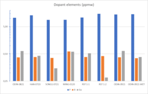
Figure 1: Content of common dopants (B, Ga and P) in different Si-kerf samples measured by ICP-MS.
Metal contamination is actually much higher than the dopant levels, due to the contamination sources in Table 1 being primarily metallic. Concentrations of the most prominent impurities are shown in Figure 2. Al can reach very high levels, up to 7000 ppm in the ODIN samples, but other samples are significantly lower, notably SONG1 below 10 ppm. There is similar Ca content (500-700 ppm) in all the dry samples. The Fe contamination varies over two orders of magnitude, but one sample, MING, is significantly higher than the rest, the common level ranging between 10 and 100 ppm. Ni from the electroplated steel wire is fairly similar between the samples, between 120 and 180 ppm, except RST 1-2, which was pre-treated, is significantly lower at 25 ppm.
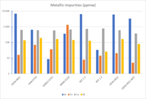
Figure 2: Content of metal impurities (Al, Ca, Fe, Ni) in different Si-kerf samples measured by ICP-MS.
For comparative purpose, five representative Si kerf samples were analysed by GD-MS. The contents of common dopant elements are shown in Figure 3, and other metal impurities like Al, Ca, Fe and Ni are shown in Figure 4. Comparing the ICP-MS results to the GD-MS results, they correlate well for most of the impurity elements. Slight difference is observed for B concentration, GD-MS give more sensitive results and low content in some samples (ODIN-0821, HAN, SONG1). The major difference is the Ga and Ca concentration. For Ga, very high values are measured by GD-MS. By checking the isotopes used in GD-MS, it is concluded that there are a lot of uncertainty on measuring Ga. Therefore, the ICP-MS results should be used for Ga content. For Ca, more than 500 ppm is determined by ICP-MS in all of the dry samples, while lower content between 20-180 ppm is measured by GD-MS. Since ICP-MS includes the sample digestion and dilution process using acids and DI water, while GD-MS measures the powder sample directly, the higher Ca content could be due to contamination. It is concluded that GD-MS data of Ca concentration is more accurate.
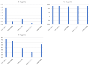
Figure 3: Content of common dopants (B, Ga and P) in different Si-kerf samples measured by GD-MS.
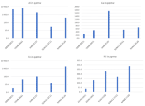
Figure 4: Content of metal impurities (Al, Ca, Fe, Ni) in different Si-kerf samples measured by GD-MS.
The carbon and oxygen content were analysed as a round robin test among three partners, and deviations were shown to be small. Average values are shown in Table 3. The typical carbon content for most of the samples is around 1-2 wt.%, while SONG1 is more than double this. The oxygen content is about 4-5 wt.%. N, S and water content of ODIN-0921 wet and dry are also shown in Table 3.
Table 3: Carbon and oxygen content measured by LECO.
| Sample-ID | RST-ODIN-0921-dry | RST-ODIN-0921-wet* | RST-ODIN-0821
|
RST-HAN-0120 | RST-MING-0120 | RST-SONG1-0721 | RST1-1 | RST1-2 | ||
| (wt.%) | ||||||||||
| Carbon | 2.0 | 2.4 | 1.8 | 2.0 | 1.0 | 4.4 | 1.8 | 1.5 | ||
| Oxygen | 4.2 | 4.5 | 5.1 | 4.3 | 4.8 | 5.6 | 4.9 | 3.9 | ||
| Nitrogen | 0.07 | 0.05 | ||||||||
| Sulphur | 0.10 | 0.15 | ||||||||
| Water (wt.%) | 0.7 | 47.2 | ||||||||
| * The wet sample has been dried before analysis. And the results shown here are the carbon and oxygen content in the sample after drying. | ||||||||||
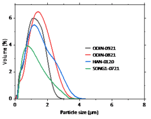
Figure 5: Particle size distribution of 4 Si-kerf samples (RST-ODIN-0921 and RST-HAN-0120).
Figure 5 shows the particle size distribution (PSD) of two representative Si kerf samples from Norway and Asia. In ODIN-0921 and SONG1-0721 samples the particles represent the smallest size. The surface area 22 m2/g and 20 m2/g for ODIN-0921 and for HAN-0120.
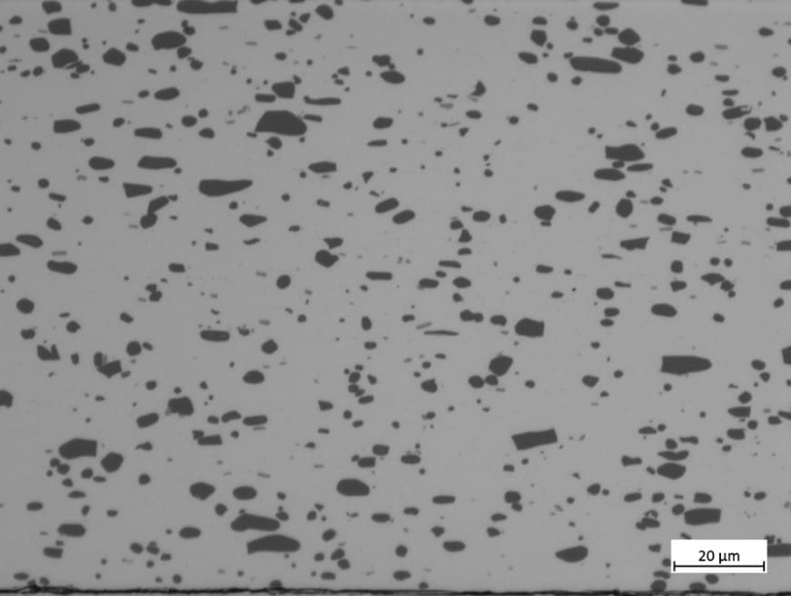
Figure 6 shows an SEM image of RST-ODIN-0921-dry Si-kerf sample. It is seen that the Si-kerf consists of ribbon-like, irregular shaped angular particles, agglomerates, and nano-sized particles. The ribbon shaped particles are up to around 4 µm long. XRD confirms crystalline silicon phase, but a broad peak around 2θ=12.5° indicates the presence of an amorphous phase.
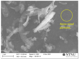
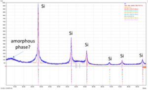
Figure 6: Top: SEM images of RST-ODIN-0921-dry Si-kerf sample. Bottom: XRD spectrum of the same sample.
The surface contamination observed by XPS for RST-ODIN-0921-dry Si-kerf sample is shown in Figure 7. Figure 7a) is a survey spectra in an area 700 um x 300 um. The main elements detected are carbon, silicon and oxygen. Small amount of aluminium is also identified, while indium is from the substrate but not from the sample. Figure 7b) is a detail spectra of silicon. The Si and SiO2 contributions can be seen clearly. Based on this spectrum, the thickness of SiO2 layer was estimated to be around 1-2 nm. Figure 7c) is a detail spectra of carbon, and there is considerable amount of carbon in the form of organic carbon. Figure 7d) is a detail spectra of oxygen. Both organic oxygen and other oxides (mainly SiO2) exist in the samples.
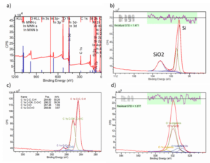
Figure 7: X-ray photoelectron spectroscopy (XPS) analysis of the RST-ODIN-0921-dry Si-kerf sample.
TEM results of Si kerf ODIN-0921 sample are shown in Figure 8. As can be seen, the morphology of the Si kerf particles can be ribbon, blocky etc. The typical size is around 1 µm while in one direction it could be very thin. Electron mapping of oxygen and silicon was performed in TEM for particles in some Si kerf samples. One example from RST-ODIN-0921 is shown in Figure 9, where green indicates the oxygen and blue indicates silicon. Based on that, the thickness of oxide layer could be measured, and it is in the range of 1-2 nm.
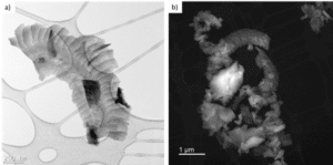
Figure 8: Bright-field TEM (a) and Annular dark-field STEM (b) images of ODIN-0921 Si kerf sample.
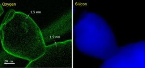
Figure 9: Electron energy loss spectroscopy mapping of oxygen and silicon in TEM for one Si particle in sample ODIN-0921.
4.2 Graphite
Graphite samples have been sorted according to their visual appearance: 1: “clean” samples, 2: yellow surface, 3: silver-grey surface, 4: silver-grey with droplet. Surface phase composition was measured by XRD on samples of type 2, 3 and 4. Only graphite was detected by XRD, while Type 2 show crystalline SiO2 and SiC phases, while type 3 and 4 show SiC and Si phases. The surface morphology of type 1 characterised by SEM is shown in Figure 10. As can be seen from the left low magnification image, there are strips on the graphite surface while the phase is homogeneous. It is further confirmed from the high magnification images shown in the right side, that only flake like graphite particles were observed. The visual appearance of type 2 graphite is shown in Figure 11 along with a SEM micrograph. The two different regions correspond to SiC (large grained structure) and SiO2 (small grained). The silicon detected on graphite type 3 are in the form of small particles on the SiC surface. The silicon on graphite type 4 forms a continuous layer with SiC crystals forming islands.
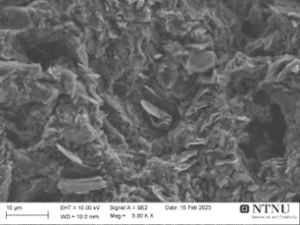
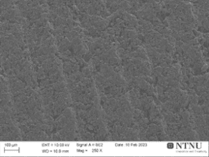
Figure 10: SEM secondary electron image of graphite type 1 sample surface.
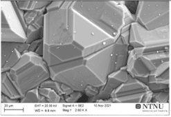
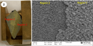
Figure 11: a) Low magnification SEM micrograph of graphite type 2 surface, the left is a photo of the corresponding sample, where there are 2 regions with different colour and thickness. Region 1 is SiC and region 2 is SiO2. b) SEM micrograph of SiC crystals on surface of graphite type 3, with small silicon particles on the surface.
Ash content was measured for all four types: Type 1 is significantly cleaner than the other types with 0.16%, vs. respectively 5.2%, 4.5% and 4.1% for the others. The ash was analysed by ICP-MS. The results are shown in Table 4; Si is the most prominent impurity, followed by Co, Ca, P, with Ni, Ti, B quite low.
Table 4: Impurity content in graphite bulk material (recalculated)
| Si | Ca | Al | Fe | Co | Ni | Ti | B | P | |
| #1 | 390 | 4.7 | 1.3 | 2.0 | 5.5 | 0.2 | 0.2 | 0.1 | 6.7 |
| #2 | 9960 | 22.3 | 0.7 | 3.2 | 34.3 | 0.5 | 0.7 | 0.2 | 0.3 |
| #3 | 12270 | 24.4 | 0.9 | 1.9 | 49.6 | 0.8 | 0.3 | 0.1 | 9.6 |
| #4 | 10900 | 21.8 | 0.6 | 2.1 | 41.1 | 0.7 | 0.3 | 0.2 | 10.2 |
The morphology and size of the graphite powder of type 1 after WC milling were also characterized by SEM and representative images are shown in Figure 12. It can be seen that there are some larger particles around 20 µm, and most of the particles are smaller than 10 µm. The shape is mostly block-like.
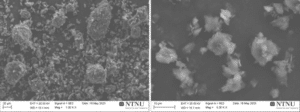
Figure 12: SEM secondary electron image of WC milled graphite powders of type 1 sample.
4.3 Silica
Silica samples were sorted according to visual inspection into the following categories: Type 1: white inner and outer surface, type 2: small yellow and black dots at the inner surface, type 3: yellow dots and extended regions on the outer surface, type 4: silver-like particles on the non-flat inner surface.
The impurity content determined by ICP-MS is shown in Table 5. The highest impurity is Ca, which is much higher than the typical amount in the new crucibles for CZ process. Co is around 21.4 ppm, which is also higher than the typical value (<0.01 ppm), which could be a result from contamination during the milling process. Similar for Fe, the samples could have been contaminated during crushing process if steel tools have been used. Comparing the 4 samples, it can be seen that type 3 has much higher Al content than the other 3, which are almost the same as in the original quartz sand and new crucible. Sample type 2 has low Fe and low P compared to the other.
Table 5: Impurity content (ICP-MS) in the 4 categorised silica samples. All values in ppmw.
| # | Na | Al | P | Ca | Ti | Fe | Co | Ba | B |
| 1 | 11.8 | 16.7 | 1.4 | 518.4 | 6.7 | 10.1 | 25.2 | 2.1 | 0.2 |
| 2 | 13.4 | 10.6 | 0.6 | 433.7 | 6.2 | 2.4 | 24.0 | 1.4 | 0.6 |
| 3 | 30.1 | 135.4 | 1.5 | 403.5 | 2.7 | 37.0 | 17.4 | 1.1 | <0.2 |
| 4 | 25.0 | 7.5 | 1.1 | 431.2 | 2.0 | 26.6 | 19.0 | 1.1 | <0.2 |
Figure 13 shows the XRD results of powder sample of silica type 4, which is similar to the pattern obtained for the other three types. A sharp cristobalite peak is observed, which is the only crystalline phase. There is a flat bump at 2θ=23o, which corresponds to the amorphous silica phase.
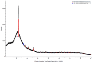
Figure 13: Powder XRD results of silica sample type 4. Same pattern was obtained for the other 3 sample types as well.
The morphology of the silica powder after milling process was also characterized by SEM for type 4 (Q-0921-t4) and Q-0722 samples, and the results are shown in Figure 14. The morphology of particles is mainly blocky. For the type 4 milled by WC, it can be seen that the particle size of the most particles is ≤ 10 um, while only a small amount is larger than 100 µm. For the mixed powder sample, the particle size of the majority is typically larger than 200 µm, which is much coarser than the one in type 4. Besides, there is also some fine particles below 10 µm.
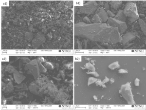
Figure 14: SEM secondary electron images of 2 silica powders after milling processes: a1), a2) Q-0921-t4; b1), b2) Q-0722.
5. Discussion
5.1 Silicon kerf
For recycling of Si kerf back into the PV value chain as new feedstock, the contamination level is an important parameter. All dopants (P, B, Ga) exist in all samples. For a recycling process of kerf back into the PV chain, choice of kerf with the same dopant as in the new product will be helpful, but not sufficient. Al is also a doping element, although not used intentionally, which comes from the cutting process. In order to avoid resistivity problems in the new material connected to this, the cutting process could be adapted, particularly the choice of beam material. The variations between the samples shows that this is a possible measure. Besides, a further refining process could also reduce the impurity level to the required amount, which is under development in the ICARUS project.
Recombination active elements like Fe and Ni come from the cutting wire itself. While Ni contamination varies only slightly, this is not the case for Fe. We have not been able to correlate the variations to process parameters due to the unknown origin of some of the samples, but different levels could result from different degrees of wire wear because of different processing conditions.
Use of Si-kerf in new products implies various processing such as drying, cleaning, refining, briquetting, pelletizing. The processability will depend on morphology and surface conditions. It is seen that some differences exist between materials in terms of particle size and surface area, although the differences are not very large. The microscopic particle morphology does not vary much between the samples, being characteristic of the fixed abrasive sawing technique, which on the other hand is very different from the morphology of the loose abrasive sawing technique used earlier. Surface oxygen varies only slightly, which is reasonable if the main source is the surface oxide being formed in contact with water or air. The surface oxide forms a protective layer preventing further oxidation, but also raise challenges for recycling in some cases. Carbon varies slightly, which could be a result of how successful the removal of the organic component of the cutting fluid has been during the post-processing. Other main contributors are organic compounds in the adhesives, in the beam and in filtration aid as well as the diamonds attached to the steel wire.
5.2 Graphite
The visual inspection appears to be a good sorting criterion for surface contamination of Si, SiO2 and SiC. Several chemical reactions involving the elements Si, C and O occur in the furnace ambient, and the balance depends on the local temperature as well as gas flows. This leads to different degrees and types of surface contamination. Elemental silicon could be the result of splashing during recharge of Si feedstock into the crucible.
The ash content is a factor 30 higher in type 2,3 and 4 compared to type 1, which again is a factor 8 higher than pure, unused graphite. The improved sampling routine for ICP-MS has shown a good distinguish between different types. The generally low levels of Ni are promising for typical graphite uses. However, the possible metal contamination (Co, Fe) in the powder milling process should be taken care of.
5.3 Silica
The differences in impurity concentration between the types are not significant, except type 3 which has an order of magnitude higher Al concentration and also much higher Fe concentration. The presence of cristobalite on the surface is confirmed for all samples.
6. Conclusion
In Si-kerf the main doping element corresponds to the added doping P, Ga, B and extra contamination. Certain metallic impurities are present in higher concentrations than the dopants, notably Fe, Ni and Al (in the order of 1000 ppmw). The contamination occurs during the sawing process, and the main contamination sources are the Ni-electroplated steel wire and the beam holding the silicon brick during wafer sawing. Again, specific concentration levels will depend on the sawing technology used by different manufacturers.
C and O light elements are in the order of 10 000 ppmw, resulting from oxidation of the kerf particles and organic residues from the cutting process. The thickness of the oxide layer was revealed to be in the order of 1-2 nm. The core of the particle consists mainly of crystalline silicon. However, there are some indications that close to the surface, an amorphous phase could be present as well. The Si-kerf particle size is in the order of 0.3 to 2.4 µm. The particle size and its distribution will depend on the diameter of the used sawing wire. Si-kerf has a relative high surface area. 1 g of Si-kerf comprises a surface area of around 20 m2.
Graphite contains mainly Si and surface infiltrations of SiC and SiO2 originating from the chemical reactions inside the furnace hot zone. Silicon droplets are present as well, which can occur through silicon recharge operations (splashing). Other detected impurities, but at much lower levels (1-800 ppmw), are Ca, Al, Fe, Cr, Ni, B, P and Ga.
Silica is mainly present in the form of amorphous silica and crystalline cristobalite. In type 4, it can contain silicon. Ca has the highest level (~500 ppmw) among other impurities. Other impurities like Na, Al, P, Ti, Fe, Co, Ba and B are also present but at much lower levels (1-40 ppmw).